Nano Dimension Combines Electronic Components within Printed Circuit Boards as part of the Printing Process
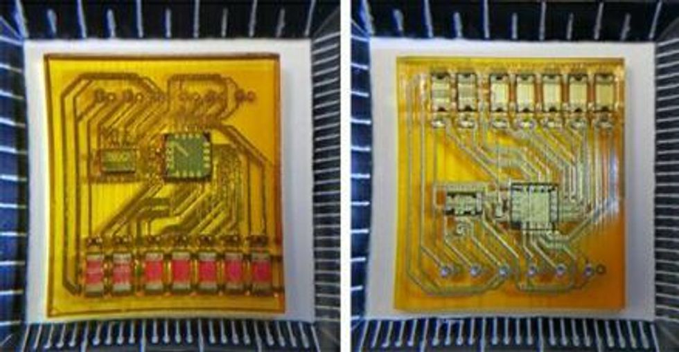
Nano Dimension (TASE:NNDM,NASDAQ:NNDM), announced today that its wholly owned subsidiary, Nano Dimension Technologies Ltd., has successfully 3D printed electrical circuits, in which it embedded electrical components, through placement, as an integral part of the printing process. The company’s 3D printer – the DragonFly 2020 – enables 3D printing of PCBs with conductive ink and dielectric ink.
Nano Dimension (TASE:NNDM,NASDAQ:NNDM), announced today that its wholly owned subsidiary, Nano Dimension Technologies Ltd., has successfully 3D printed electrical circuits, in which it embedded electrical components, through placement, as an integral part of the printing process. The company’s 3D printer – the DragonFly 2020 – enables 3D printing of PCBs with conductive ink and dielectric ink.
Today, the company announced a successful proof of concept of PCBs inkjet printing, in which electrical components were placed during the printing process. The method presents several advantages:
- It improves the PCB reliability by maintaining the electronic components internally and keeping them from being exposed to the external environment, while protecting them from mechanical, temperature, and corrosion damages.
- It makes obsolete the soldering process since the components are embedded within the printed board during printing. The connectivity between components then takes place as part of the 3D printing process without the need for a mediating soldering material.
- The new process enables printing on electronics components without their complete packaging (printing directly on the dye), and consequently supports the creation of thinner, more protected PCBs.
This new and significant capability is expected to become supported in future versions of Nano Dimension’s 3D printers.
The company has filed a patent application with the U.S. Patent and Trademark Office for this unique development, which the company believes is significant for a wide range of industry sectors such as defense, space, consumer products, telco, and more.
About Nano Dimension Ltd.
Nano Dimension, founded in 2012, focuses on development of advanced 3D printed electronics systems and advanced additive manufacturing. Nano Dimension’s unique products combine three advanced technologies: 3D inkjet, 3D software, and nanomaterials. The company’s primary products include the first 3D printer dedicated to printing multi-layer PCBs (printed circuit boards), and advanced nanotechnology-based conductive and dielectric inks.
In addition to the trading of the company’s American Depositary Shares on NASDAQ, the company’s ordinary shares are also traded on the TASE in Israel. The Bank of New York Mellon serves as the depositary for Nano Dimension.
Forward-Looking Statements
This press release contains forward-looking statements within the meaning of the “safe harbor” provisions of the Private Securities Litigation Reform Act of 1995 and other Federal securities laws. Words such as “expects,” “anticipates,” “intends,” “plans,” “believes,” “seeks,” “estimates” and similar expressions or variations of such words are intended to identify forward-looking statements. For example, we are using forward looking statements in this press release when we discuss the potential and possible uses of our products, that future versions of our printers will support certain printing capabilities and the market opportunity for our products and new technologies. Because such statements deal with future events and are based on Nano Dimension’s current expectations, they are subject to various risks and uncertainties. Actual results, performance or achievements of Nano Dimension could differ materially from those described in or implied by the statements in this press release.
In addition, we cannot assure that any patent will issue as a result of a pending patent application or, if issued, whether it will issue in a form that will be advantageous to us. The forward-looking statements contained or implied in this press release are subject to other risks and uncertainties, including those discussed under the heading “Risk Factors” in Nano Dimension’s prospectus filed with the Securities and Exchange Commission (“SEC”) pursuant to Rule 424(b)(4) on September 27, 2016, and in any subsequent filings with the SEC. Except as otherwise required by law, Nano Dimension undertakes no obligation to publicly release any revisions to these forward-looking statements to reflect events or circumstances after the date hereof or to reflect the occurrence of unanticipated events.
